Nordic pellicles: a tiny and important thing for semiconductors
Teeny tiny pellicles are helping us make the world's smallest chips
What do the happiest place in the world, the coolest prime minister, a place where decaf coffee is almost non-existent, snow, and a tech powerhouse have in common?
If you guessed Finland, well done. You’ve clearly been reading the news!
Shaped by centuries of geopolitical events, Finland has developed a distinctive culture of open collaboration and self-sufficiency in almost every aspect of life. Take strategic stockpiling of goods as an example. Each year the heads of the largest companies from industries as diverse as telecoms, food and fashion meet to discuss contingencies. This platform of cross-fertilisation has nurtured a real focus on innovation.
On top of this, Finland’s education “miracle” and its emphasis on play, problem-solving and freedom for children to choose what they learn from a young age means, today, some of Finland’s greatest assets are their engineers and R&D prowess.
Situated at a strategic confluence of East and West, empires came and went — yet Finland still stood, resolutely. So much so that when Finnair, the nation’s flagbearer, had to think hard about adjusting flights to Asia in light of the Ukraine situation, the government said “Finnair is of vital importance for Finland… if you look at the map, Finland is practically an island.”
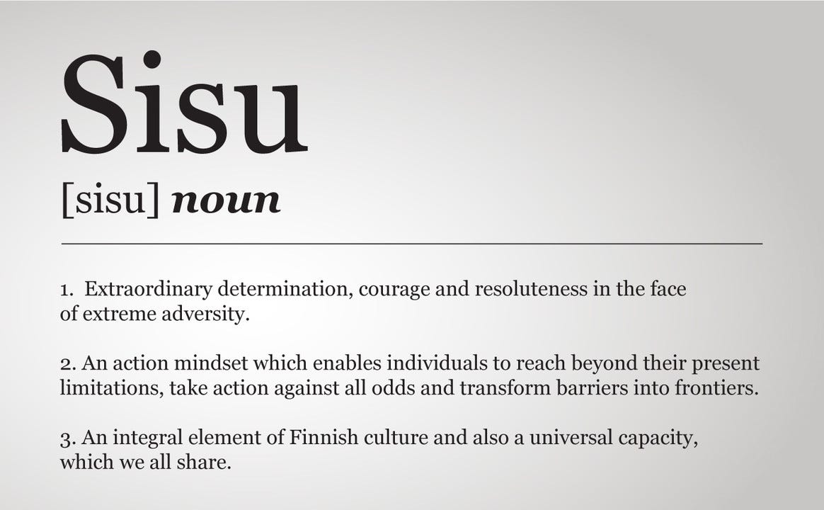
In fact the Finns have a something called “Sisu”, a saying which relates to survival and success.
Perhaps this goes some way to explain Finland’s penchant for coming up with technological novelties and persevering with them.
Which begs a question - what is the hottest topic in technological self-sufficiency that comes to mind these days? If you guessed semiconductors you’d be spot on — and if you guessed EUV lithography technology, even more so.
A short history of EUV lithography and why it is so significant
Public interest in EUV lithography has been red hot over the past few years. To explain why this is so important, we have to step out of Finland for a moment and into a town deep in the southern industrial heartland of the Netherlands.
Like all great companies, ASML Holding N.V., originally short for Advanced Semiconductor Materials Lithography, began life in a shed.
Born in 1984 as a joint venture between ASM International and Philips to address burgeoning market for semiconductor lithography machines dominated by Japanese players such as Nikon and Canon. Their HQ in Veldhoven is merely a 15-minute drive from Philips in Eindhoven, after all.
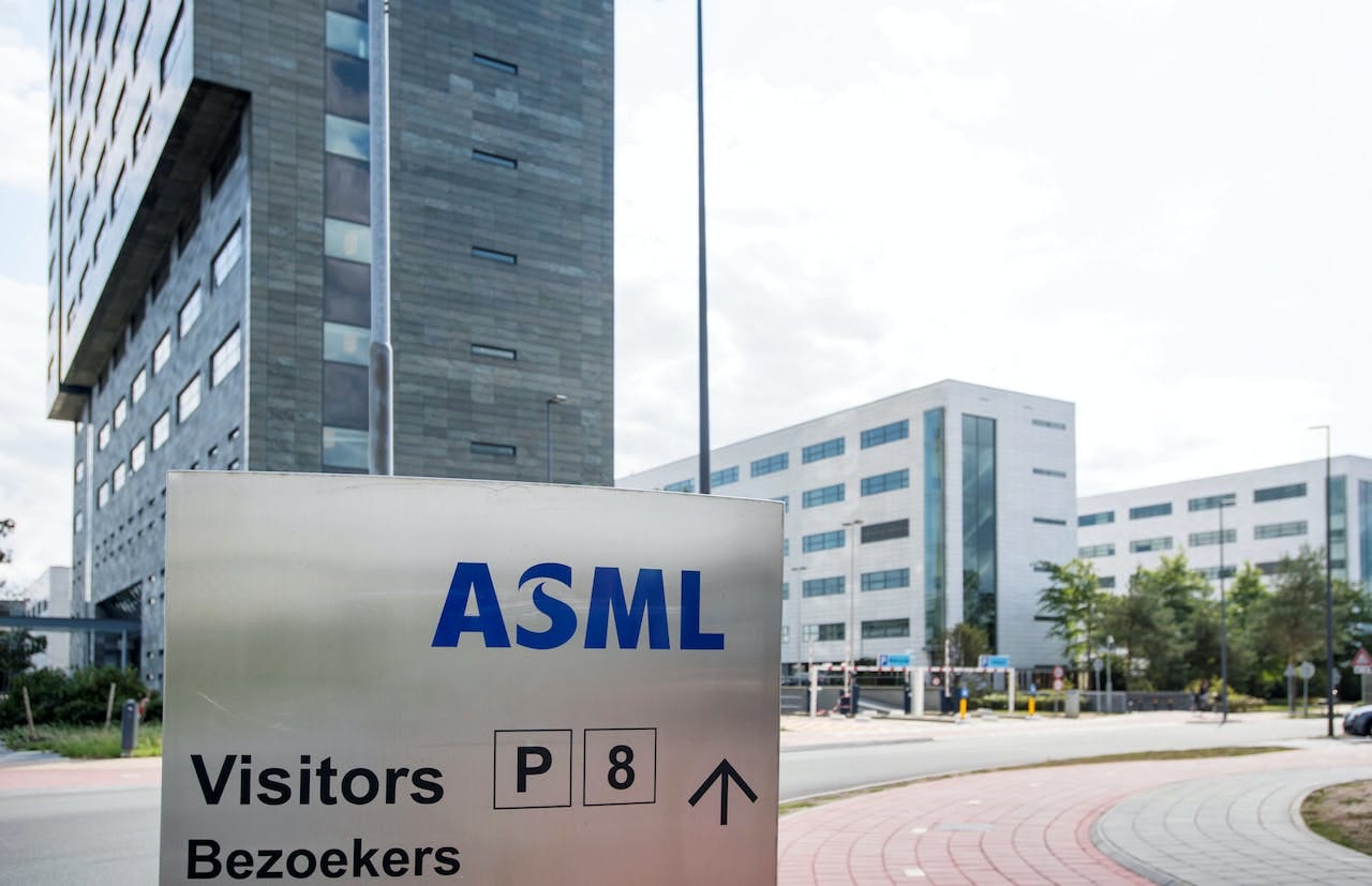
Publicly listed since 1995, today ASML is the unquestionable market leader in lithography machines worldwide, turning over EUR18bn in 2021 with a >EUR200bn market cap as at time of writing.
As much as I would like to write all about ASML’s interesting history, there are plenty of great write-ups, some of which you can find here, here and here.
The market has gone bananas for ASML’s Extra Ultraviolet Lithography (EUVL) technology which uses an extremely narrow wavelength of light (13.5nm) to fabricate chips 7nm and under. Finally in commercialisation, these machines are are sold out years in advance, and retail for between USD130 million to over USD300 million each!
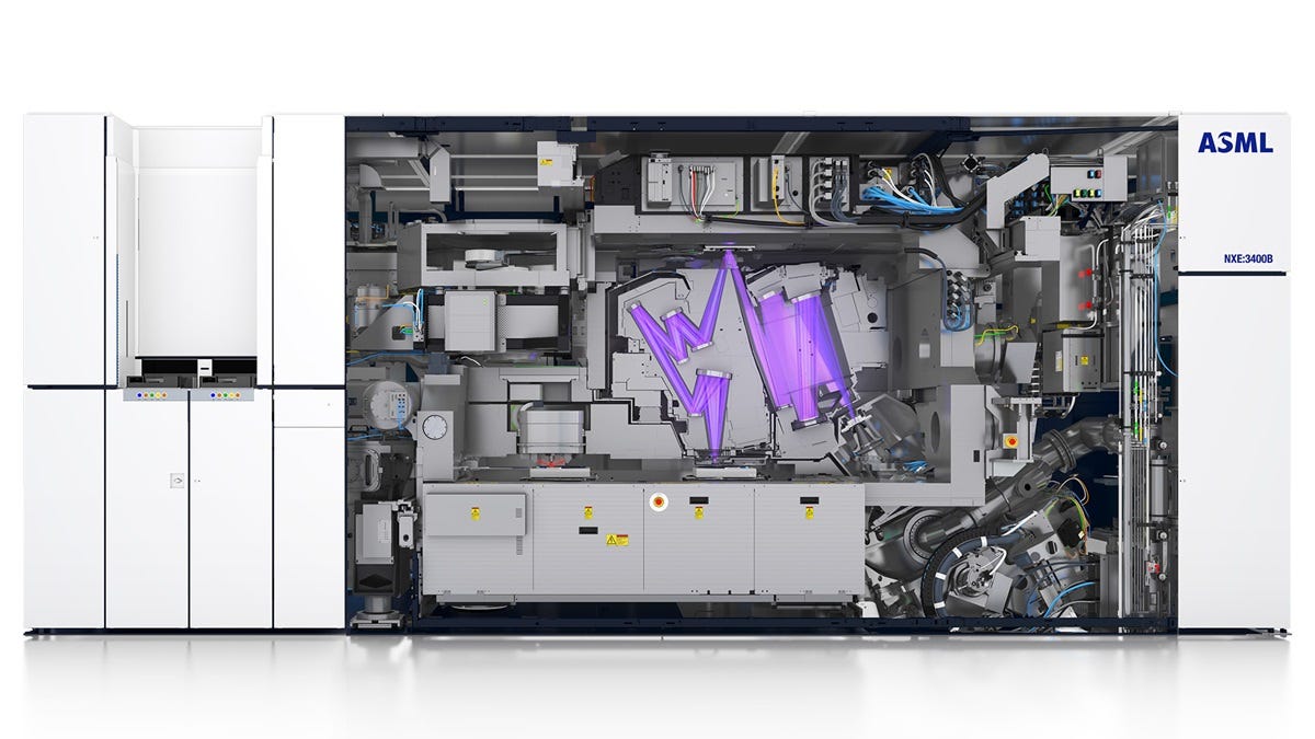
With over 100,000 components going into EUVL machines, EUVL has been peppered with “0 to 1-type” engineering challenges throughout its development history. Starting from over a decade ago, many had already been hoping the tech would have been commercially rolled out already, but by 2010 ASML had only just released their EUVL prototype, the TWINSCAN NXE:3100.
With all the hype around EUV, it’s easy to forget ASML’s cash cow — their range of dry and wet lithography Deep Ultraviolet machines. After the technology started to emerge in the 1990s, ASML worked with the leading chipmaker, TSMC, to develop a 193nm-based excimer laser DUV solution. ASML has competitors in DUV (Nikon in wet lithography, Canon in dry), but they still dominate overall.
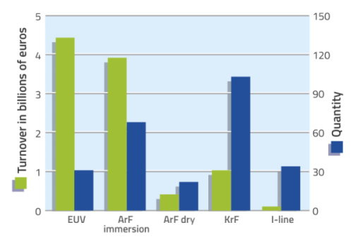
Though not as pricey as EUV, these machines still cost anywhere between EUR10 million to EUR60 million. They still form the backbone of the semiconductor fabrication industry — in fact the high demand for DUV machines has been severely underestimated.
It’s helpful now to lift the lid a little on how this key step in the chip-making process came to be.
A quick journey through the development of semiconductor lithography
In basic terms, the key part of making chips (fabrication) is via a process called photolithography, which uses light to react with chemicals on a silicon wafer through a photomask containing the chip design.
Amongst advanced photolithography processes used for high volume chip fabrication, the most widely used process is Deep Ultraviolet lithography (DUV) with excimer lasers (produced by Cymer in the US, which ASML acquired in 2013) at wavelengths of 248nm (Krypton fluoride) and 193nm (Argon fluoride), which can create over 6,000 wafers per day. These machines are used by all the major chip foundries (TSMC, Samsung, UMC, GlobalFoundries, SMIC you name it).

The age-old debate in the semiconductor industry has been around Moore’s Law, an observation in 1965 by semiconductor legend Gordon Moore that the number of transistors in a dense integrated circuit doubles about every two years. The more transistors there are on a chip, the more computing power it can offer. After holding true for many decades, the observation is now under pressure.
One of the key formulae used in the industry to push forward Moore’s Law is the Rayleigh Criterion for resolution of chips. At a basic level, to make chips smaller (CD) and smaller one needs to work on making the numerator, wavelength, smaller (λ), or the denominator, numerical aperture (NA), larger.
In 2003, ASML made a breakthrough called immersion lithography which significantly increased NA. This is where light is projected through a layer of highly-purified water to increase the refractive index beyond one (e.g. 1.44 for 193nm DUV lithography) which increases resolution by a similar factor. This technique is used in all of ASML’s advanced lithography machines.
You will hear about chips getting smaller and smaller and into the single digit nanometres but, in reality, doing anything below 20nm is extremely difficult without another technique called multiple patterning. Despite even this development, DUV began to hit a wall 🧱 (I have left a layman’s explanation of it here).
EUV comes rolling in 💡
Entirely unique to ASML, EUV lithography systems are some of the most complex machines ever built.
The main premise is their use of 13.5nm EUV light (a wavelength 14 times narrower than DUV) to shrink λ in order to decrease CD. Since EUV light basically does not exist on Planet Earth, something almost physics-defying occurs to generate it. A CO2 laser is blasted at a liquid tin droplet around 25µm in size, not once, but twice. The first shot primes the tin droplet into pancake shape, and then the second, more powerful beam, pulverises it into EUV light-emitting plasma. This process is repeated 50,000 times a second (!!!) to generate sufficient light exposure. It is simply amazing.
Since EUV light has such a narrow wavelength and is absorbed by everything, conventional lithography optics using lenses would absorb all of the EUV rays. Instead, the system relies on a series of ultra-smooth mirrors containing over 100 layers of materials polished to a smoothness of less than one atom’s thickness to maximise light reflected onto the wafer.

Since reflectance is so important for EUVL, photomasks have had to be re-engineered. This has created both a huge opportunity and huge headache for photomask makers.
Moreover, EUV light is actually shone at a 6-degree angle in order to prevent incident and reflected light from overlapping, and as with most other things associated with the EUV revolution, photomasks have not been spared an overhaul!
Unlike traditional optical photomasks that transmit light, EUV photomasks aim to reflect light. To reflect as much light as possible some of the most expensive metals (think ruthenium, molybdenum, tantalum, not your household names) around are stacked together to create photomasks with reflective and absorbing regions to create the desired design image on the wafer.
All of this is big news, and so is the price tag, around 3-times dearer at $300,000 a piece. Not only do these photomasks need to be cleaned properly from time to time, the change in technology also makes mask inspection and defect repair tougher and more expensive than before.
The number of photomasks required for EUV are fewer than what would have been needed if DUV multi-patterning approaches were used for advanced nodes. Still, since semiconductors are fabricated with multiple design layers, photomasks traditionally come in sets which have comprised anywhere between 5 to >70 individual photomasks depending on the type of chip technology being used. You start to see how important it is to have photomasks in good working order.
But what if photomasks get damaged? 🤔
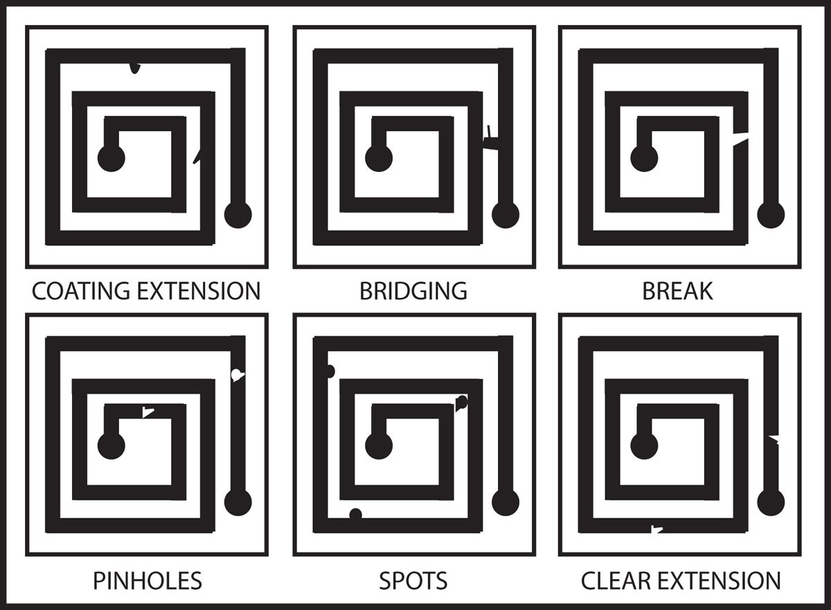
The challenges with scaling EUV lithography seem to be with, well… everything 😆
Originally, the industry thought the clean-room type environment of EUV systems would prevent any particles from damaging their precious photomasks — alas, they quickly realised this was not to be. It turns out smashing a high power laser beam into a drop of tin causes particles to fly everywhere and makes EUV lithography a dirty business, literally!

So although replacing four steps of DUV with one EUV step looks to have improved the defect rate and speed of yield learning at advanced nodes like 5nm, EUV lithography is still in “yield infancy” (Samsung’s for their 5nm chips is reportedly as low as 35%).
It turns out some of these issues can be addressed by something incredibly thin and seemingly innocuous.
Pellicles: indistinguishable from magic
In September, ASML placed an article on their landing page, front-and-centre, about the “magic” of EUV pellicles, talking about the many trials and tribulations to finally get to a suitable pellicle solution offering 90% transmissivity, and made no doubt about their significance to the value chain. This is undeniably a great breakthrough and starting point for mass EUV chip fabrication1.
What are pellicles? Why are they needed for EUV lithography?
A pellicle is a very thin, transparent layer which is mounted above the patterned side of the photomask and protects it during the chip fabrication process.
Pellicles need to be transparent enough to allow light from the lithography machine to be transmitted onto the photomask (reticle), yet durable enough to withstand the harsh EUV conditions (heat, plasma etch etc.).
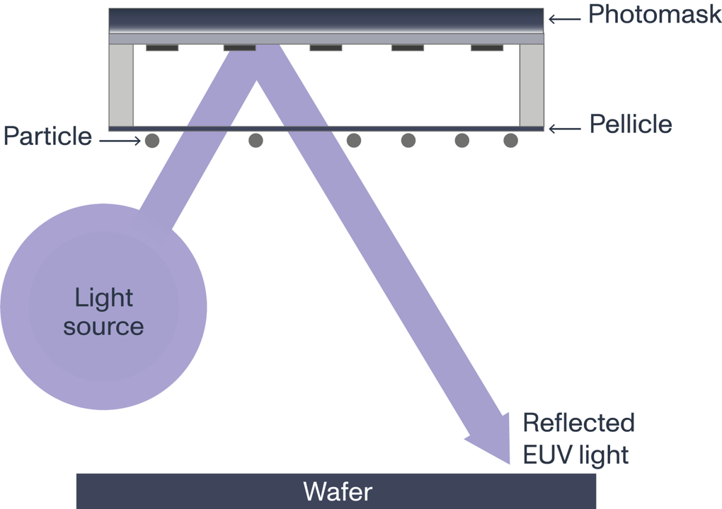
Although the most interesting aspect might be the pellicle membrane and the material with which it is made, it is actually comprised of a whole system, including a frame, fasteners, support pod and pellicle changing machine.
Pellicles are important, and there are a few key reasons why. One is so that the photomask is protected from particles depositing on it, second, that particles depositing on the pellicle are out of focus enough to not affect the wafer pattern.
ASML has created an entry point pellicle suitable for mass volume manufacturing, but what else is out there? Word on the street is ASML will continue outsourcing pellicle development to vendors, since the industry would prefer they stick to their (amazing) bread-and-butter scanners.
Everyone is hung up about EUV transmission %
It goes without saying, the more transmissible it is the better. The EUV beam needs to pass through the pellicle twice for a reflective photomask, so the more the beam is attenuated, the longer the wafer needs to be exposed to achieve a fixed dose, leading to lower wafer throughput. Pellicles prototyped to date lose between 11% and 20% in absorption of EUV light for a single pass through the wafer (so EUV transmission is only 80-89%). With ASML’s EUV machines costing $130m to >$300m a pop, this poses a significant dent on your ROI.
So now ASML has finally rolled out pellicles made of metal silicide which have achieved the 90% transmissibility benchmark for mass volume manufacturing.
The reality is the industry expects much more than just 90% (and not just this but many other things as well). Turns out there aren’t really any materials out there that can top this… except… well… carbon nanotubes.
Carbon nanotubes and Canatu
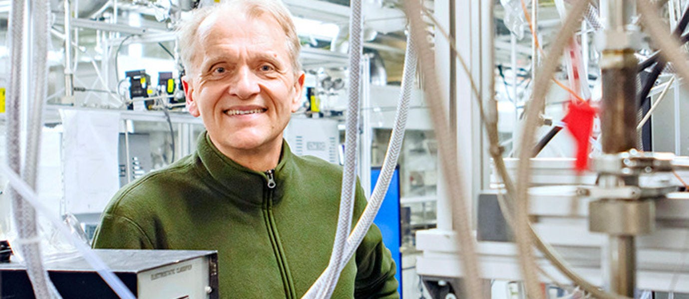
An explosion of innovation has occurred on the outskirts of Helsinki, the Finnish capital. Otaniemi, once an expanse of farmland along a marine area known for its bird habitats, is now home to some of the best technology businesses Finland has ever produced (think Kone and their elevators, Nokia and their mobile phones, and Rovio with Angry Birds). It is also home to Aalto University and its award-winning nanotechnology department. It is here that Canatu spun out in 2004 from research on carbon nanotubes (CNTs) by UNESCO Nanosciences Medal winner Professor Esko Kaupinnen and several of his colleagues.
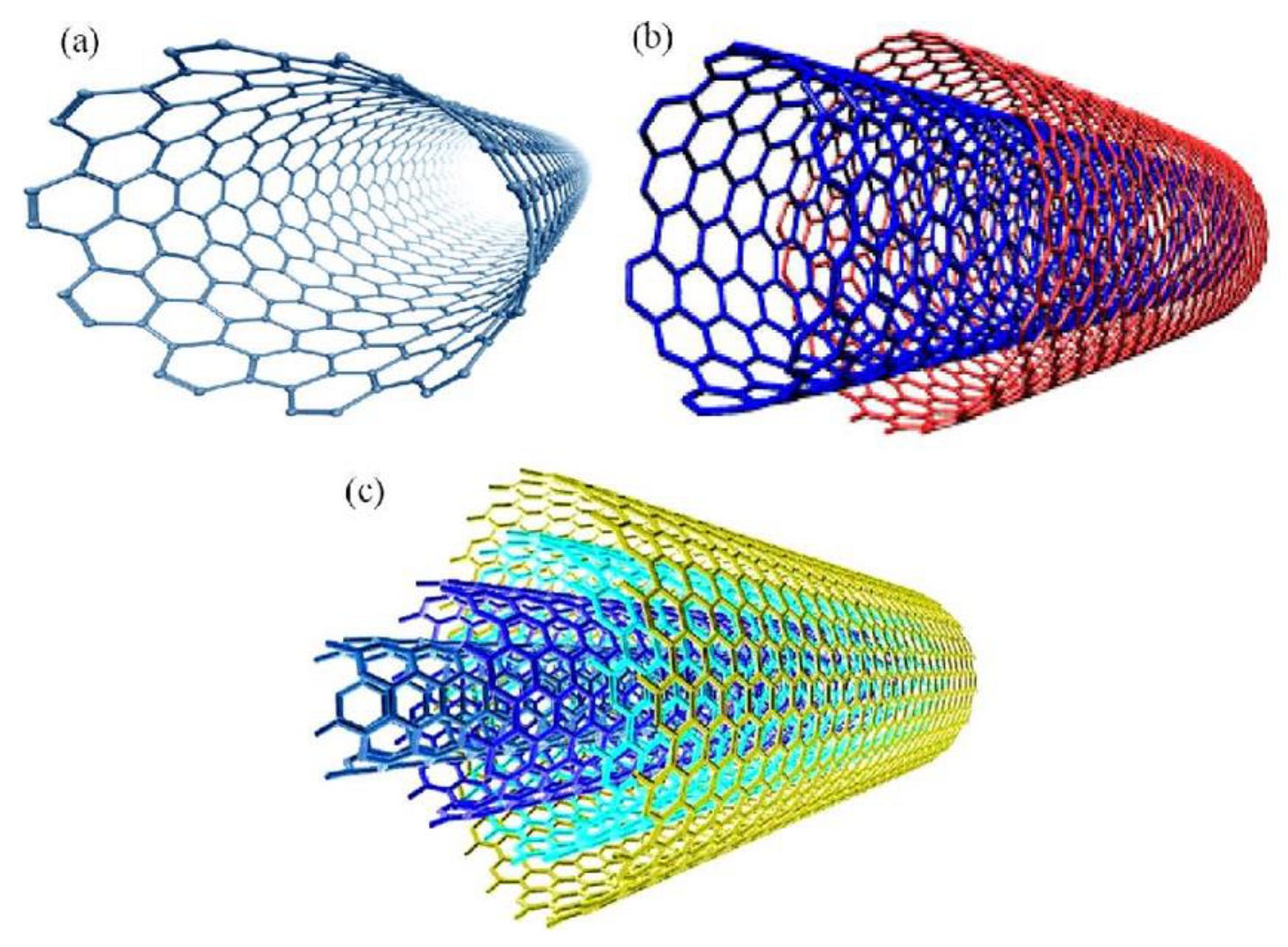
Carbon nanotubes (CNTs) are essentially rolled-up tubes of graphene which are up to several nanometres wide.

They can come as single-walled, double-walled or multi-walled structures, with trade-offs in size, durability, pliancy and functionality.
Sometime during 2016, imec, the watering hole of the semiconductor industry, approached Canatu to ask about their CNTs and to start a collaboration. IMEC was in fact founded at the same time as ASML in 1984, just across the border in Belgian Flanders, to encourage collaboration and knowledge-sharing in the microelectronics industry. The two have much to thank each other for their multi-decade success stories.

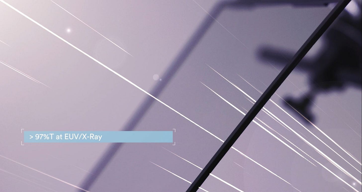
In 2020, Canatu’s CNTs were first tested on ASML’s EUV Twinscan NXE:3300 machine at imec’s facilities to demonstrate fabrication and scanner handling of full-sized CNT pellicles. Canatu’s CNTs have demonstrated 98% transmissibility - that’s right, 98%! This translates into an increase in wafer throughput resulting from shorter lithographic exposure times.
What ensued was a flurry of activity of relationship-building with the broader semiconductor ecosystem.
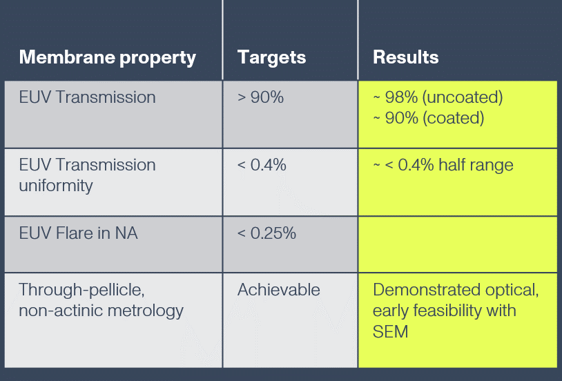
CNTs are demonstrating many unique advantages as pellicles
The advantage of CNTs really stems from their tunability since it turns out the adjusting the number of CNTs in a membrane modify physical properties like strength and gaps between tubes and also the desired transmission and emissivity.
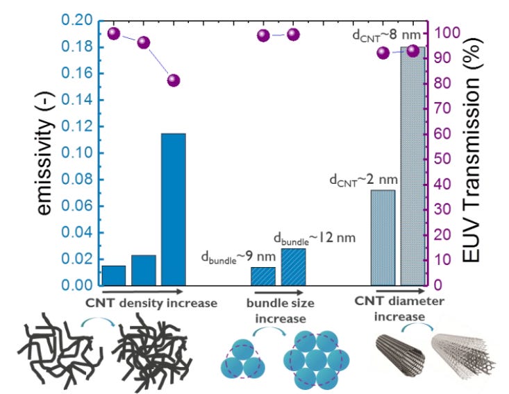
Emissivity is important because EUV light at high powers (>400W) will heat the thin membranes to temperatures on the order of 600C to 1000C. For these thin membranes in vacuum, the primary mechanism for heat dissipation is through emission.
They are strong enough to cover a 6’’ x 6’’ photomask and maintain their tensile strength even in rapid heating and cooling conditions.
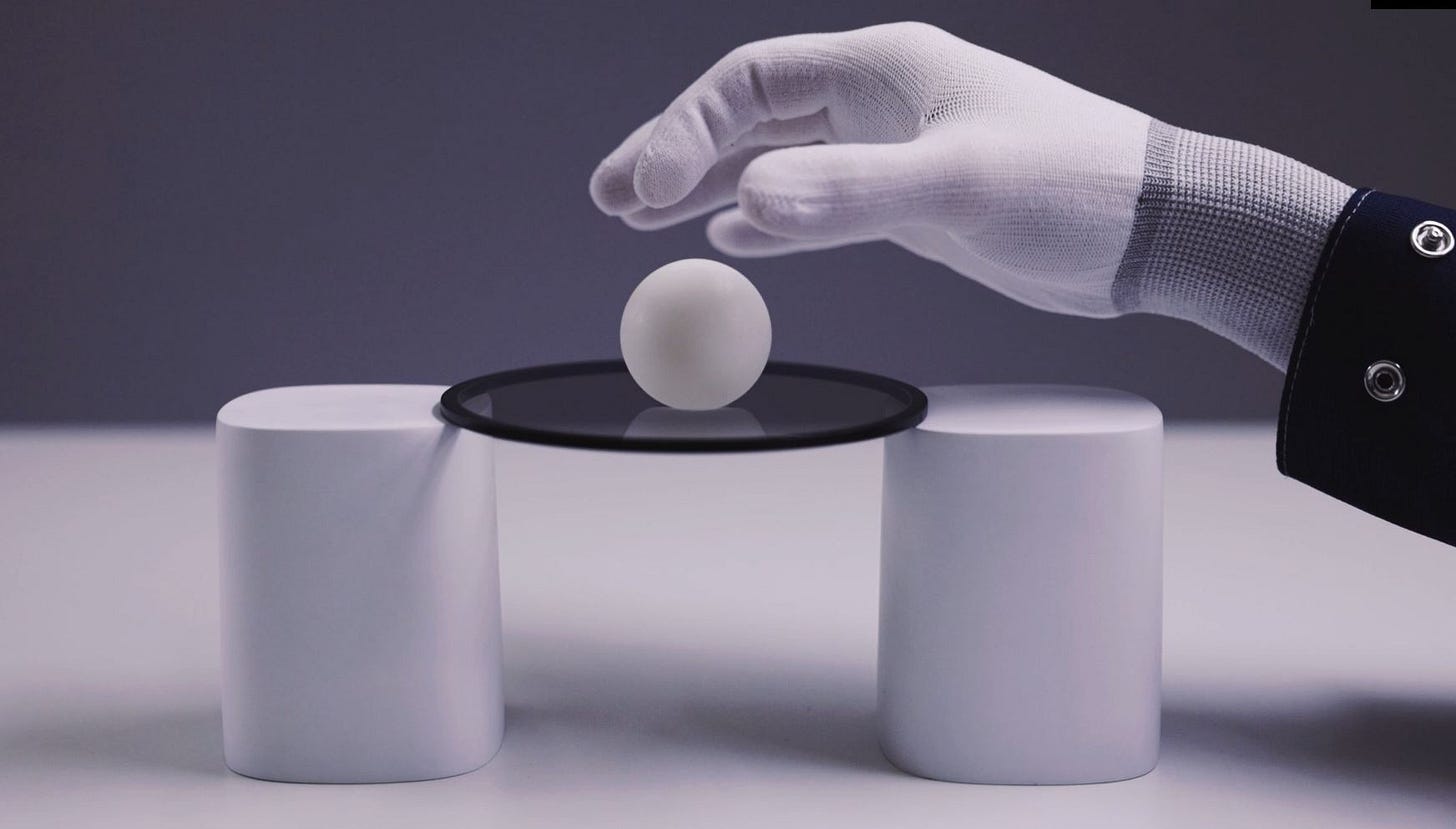
CNT pellicles need a coating to prevent etching from hydrogen plasma in the extreme EUV environment. This coating will decrease the EUV transmission over uncoated CNTs, but can be designed via material and thickness to enable a pellicle solution that remains well above the 90% EUV transmission target.
Crucially, their unique properties mean CNTs allow photomasks to be inspected by existing actinic metrology machines such as those used for DUV since they allow 193nm light to pass through without needing the system to be dismantled for the purposes of inspection.
Canatu’s superior CNT manufacturing prowess

At a basic level, CVD works by passing hydrocarbon vapour through a synthesis reactor containing catalyst material at high temperature (600-1200C). The CNTs then form on the catalyst in the reactor and are collected after being cooled to room temperature.
Conventional CVD has its drawbacks since it involves several complicated steps to spray wet CNT particles onto a substrate (wet dispersion), lowering uniformity and structural integrity of the CNTs and reducing their strength and functionality. Heavy use of methane-, acetylene-, benzene-based catalysts means it’s not environmentally friendly either.
Instead, Canatu has perfected a method of dry deposition, using Floating Catalyst Chemical Vapor Deposition (FC-CVD). Metal catalyst vapour is essentially heated and synthesised with the hydrocarbon gas, allowing CNTs to grow in-situ on the catalyst vapour and form perfectly by the time they deposit on the substrate.
What’s great is Canatu’s process works very well for mass manufacturing, and they now have a fully-automated production line which has since expanded capacity 150 times in a new factory equipped with state-of-the-art cleanrooms which can quickly ramp-up to meet industrial demand levels.
CNTs really are a feat of scientific ingenuity, and you’ll be fascinated to know about what else they can be used for here.
EUV and pellicles: what do the next few years have in store?
Two pieces of public information from ASML have been quite insightful.
The 2021 annual report of ASML looks very interesting if we analyse how their EUR18.6bn in sales is made up.
>90% of sales were to Asian customers
Segment-wise, by 2030, smartphones are expected to remain the largest at $210bn, but automotive (16.3%) and industrial electronics (10.5%) are forecast to have the highest 2020-2025 CAGRs driven by demand for artificial intelligence, sensor processing and GPUs
And based on ASML’s Q3 2022 earnings call, the feeling is customers are still urgently pushing ASML, with 85% of the order book for advanced immersion lithography machines that make the smallest chips, so that they can get cracking with ASML’s prized DUV and EUV machines. ASML even revised up their 2025 demand forecasts for DUV (260 to 600) and EUV (53 to 90) machines, including 20 0.55 high NA machines in the medium term. So it looks like pellicles will be flying off the shelves too!
Geopolitical and consumption trends aside, Asia is a key driver of demand, and tech innovation and sovereignty look set to dominate customers’ agendas. Chips are said to be the new oil. Globally-minded European tech companies like ASML and Canatu are well placed to take advantage of this trend.
ESG considerations
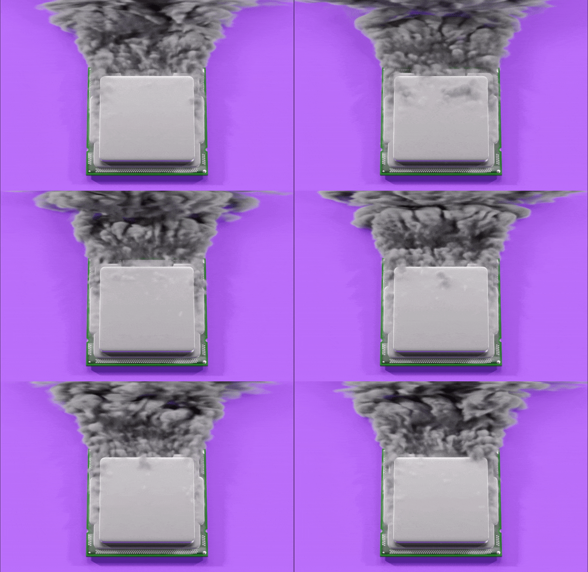
EUV machines are said to consume 1 MW of electricity, which is 10 times more than DUV and other lithography machines. By 2025, TSMC, ASML’s largest customer for EUV machines, is expected to consume 12.5% of Taiwan’s electricity as a consequence.
ASML already has a significant ESG agenda to improve the system energy efficiency of their EUV systems to reduce energy consumption by 10% from their 1.4MW 2018 baseline.
A 25% improvement in production efficiency on the wafer means Canatu’s CNT pellicles will go a long way towards helping ASML with this.
Conclusion: don’t forget Mr. Pellicle — he’s bloody important!
It may be bizzare to say this, but having persevered through plenty of challenges to finally engineer a breakthrough, the little-known, and seemingly innocuous pellicle may very much have… Finnish DNA. Oh Sisu ❄️
Given the importance of pellicles to the future of semiconductors, it’s fair to say Canatu and Finnish innovation have found yet another way to carve out a successful niche.
So whilst there are plenty more exciting topics we should also cover in semiconductors, let’s not forget the humble yet impressive, Mr. Pellicle. 🎩
Bits and pieces that are also great to know (an appendix, of sorts!)
If Canatu’s CNTs are so great, what else can they be used for? 🤔
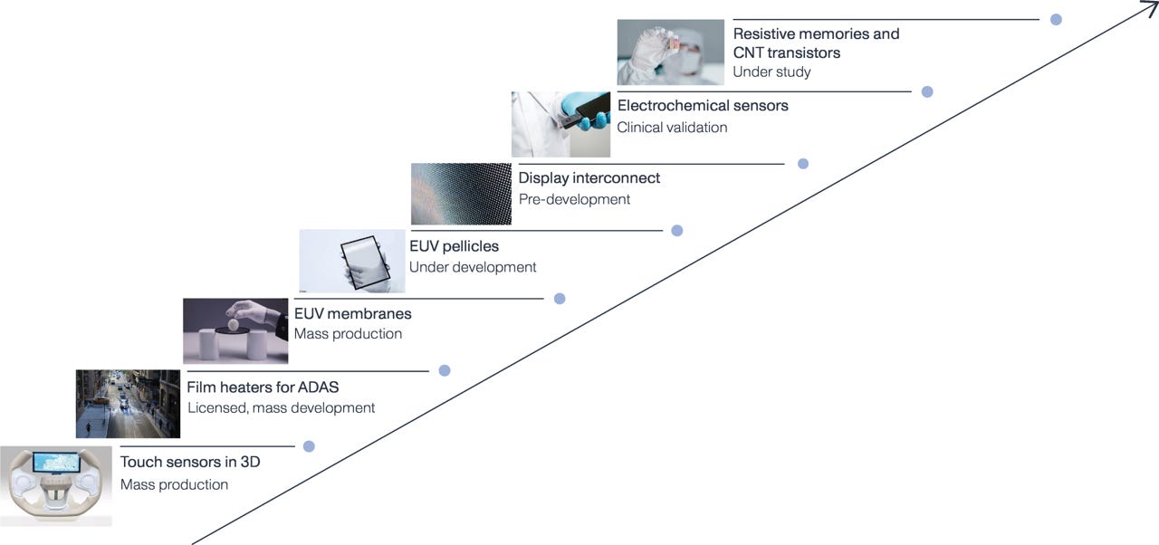
CNTs are inherently versatile. Take a quick look at Canatu’s website and you’ll see how.
CNTs can be up to 180,000 times thinner than a human hair in diameter yet stronger than steel per unit weight. They are 10 times stronger than your iPhone screens, are highly conductive and functional, and are optically very clear — perfect for all sorts of smart consumer electronics including stretchable displays.
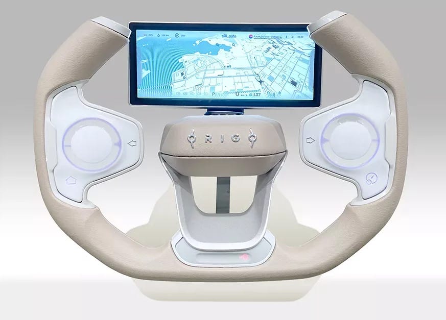
Since CNTs are so stretchable and shapeable, they are well suited to replacing traditional mechanical buttons in automotive interiors and controls constructed with multiple layers which pick up wear and tear easily over time. Canatu’s products can replace the hardware stack with one, intelligent and functional 3D film.
When the sheet resistance of the CNTs is increased, they can become excellent transparent heaters, perfect for heating lidars, cameras and windshields for automotives of the future. They also consume 1/10th of the energy of conventional heaters.
Because of Canatu’s unique dry deposition method, their CNTs have highly electrochemically active surface areas which are ideal for biosensors. This means we could expect point-of-care blood test solutions using CNTs in the near future, not just indicating the presence of something (e.g. opioids), but also how much of it and how concerned we should be about it.
CNTs even have the potential to help us see further into space by filtering out X-rays.
Most importantly, awareness of CNTs is now reaching the mainstream. Carbon nanotubes are now being taught to 14-15 year olds now at school!
Canatu’s CNT products are really leading the race in functional versatility.
A layman’s overview of multi-patterning (why DUV hit a wall) 🧱
You will hear about chips getting smaller and smaller and into the single digit nanometres, but in reality doing anything below 20nm is extremely difficult without something called multiple patterning.
The basic premise of multiple patterning is to increase line (pattern) density by shrinking the distance between two lines on a chip by overlaying more lines in between them. Originally this was done by subjecting the wafer to two or more lithographic exposures using multiple photomasks, combining and superimposing the patterns to create a much higher resolution image on the wafer (see the Litho-Etch-Litho-Etch (LELE) process). Up to a certain point, this can be repeated many times, which leads to:
Multiple patterning today has moved towards spacer patterning, often termed Self-Aligned Double Patterning (SADP). The key difference versus LELE is pitch splitting (making line distances smaller) is achieved through spacers (aka dummy lines), which help avoid issues with aligning photomasks lithographic exposure only occurs once. You end up with much better CD uniformity. Although the SAPD process also uses different photomasks in the process, the first mask contains the entire design (the dummy pattern), whereas the second mask sits below the layer of spacers so that it can be etched into the final design with smaller pitch and greater density. It’s a bit less intuitive to understand, I know, but it’s worth getting your head around it as this is where the industry is headed.

A layer of dielectric (in green) is deposited over the dummy pattern, after which it is chemically etched away leaving spacers (also known as sidewalls) for patterns to be created based on them. Whether it is LELE or SADP, both introduce complexity into the process, making things more tedious and expensive. This is because number of steps in production have to increase, which also means debugging of the chip design becomes more difficult.
By the time DUV lithography processes started tackling the 7nm node they had to multi-pattern four times (quadruple patterning, or SAQP), a headache which basically meant doubling the steps of SADP. In terms of making chips smaller, DUV started to hit a wall.
Was this article on semiconductor EUV pellicles useful? Help me to improve!
With your feedback, we can improve the letter. Click on a link to vote:
Build your own? 👉 FeedLetter.co
All views contained in this article are my own and do not necessarily represent the views of any other organisation.
None of the above constitutes investment advice in any way.
Canatu Oy is a portfolio company of Ascend Capital Partners.
ASML’s pellicle has been subcontracted to Mitsui to manufacture.


